Xiamen Tmax Battery Equipments Limited was set up as a manufacturer in 1995, dealing with Laboratory equipments, technology, etc. We have total manufacturing facilities of around 2, 000 square meters and more than 100 staff. Owning a group of experie-nced engineers and staffs, we can bring you not only reliable products and technology, but also excellent services and real value you will expect and enjoy.
Sputter Coater: A Professional Overview of Advanced Thin-Film Deposition Equipment
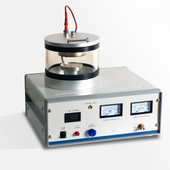
Overview
A Sputter Coater is a critical piece of vacuum-based deposition equipment widely used in materials science, microelectronics, surface engineering, and analytical sample preparation. Its primary function is to deposit a thin, uniform layer of conductive or functional material onto a substrate by means of physical vapor deposition (PVD). By utilizing plasma to eject atoms from a solid target and condense them onto a surface, a sputter coater enables precise control over film thickness, composition, and adhesion. Due to its versatility and reproducibility, the sputter coater has become an indispensable tool in both research laboratories and industrial manufacturing environments.
Key Features
Modern sputter coater systems are designed with a combination of precision engineering and advanced control technologies. One of the most notable features is the high-vacuum chamber, which minimizes contamination and ensures high-purity film deposition. Many systems support multiple target materials, allowing users to switch between metals, alloys, and compounds with minimal downtime.
Additionally, sputter coaters often incorporate adjustable power supplies (DC, RF, or magnetron), enabling compatibility with both conductive and non-conductive targets. Automated control panels or touchscreen interfaces allow users to accurately set parameters such as sputtering power, gas flow rate, deposition time, and chamber pressure. Some advanced models also include substrate rotation, heating, or biasing functions to improve film uniformity and adhesion.
Working Principle and Process
The sputtering process begins by evacuating the chamber to a high vacuum level, typically using a combination of rotary and turbomolecular pumps. Once the desired vacuum is achieved, an inert gas—most commonly argon—is introduced into the chamber. A high voltage is then applied between the target (cathode) and the substrate (anode), ionizing the gas and forming a plasma.
Argon ions are accelerated toward the target surface, where their impact causes atoms from the target material to be physically ejected. These ejected atoms travel through the vacuum environment and deposit onto the substrate, forming a thin film. The deposition rate and film properties can be finely tuned by adjusting parameters such as power, pressure, and target-to-substrate distance. This controlled process allows sputter coaters to produce films ranging from a few nanometers to several micrometers in thickness.
SEM Sputtering Coater
Applications
The Sputter Coater is widely used across multiple industries due to its adaptability and precision. In scanning electron microscopy (SEM), sputter coaters are essential for coating non-conductive samples with a thin conductive layer, improving image quality and reducing charging effects.
In the semiconductor and microelectronics industries, sputter coaters are used to deposit metal interconnects, barrier layers, and electrode materials. In optics, they enable the fabrication of reflective, anti-reflective, and interference coatings on lenses and mirrors. Additionally, sputter coating plays a key role in the production of thin-film sensors, photovoltaic devices, magnetic storage media, and biomedical coatings.
Advantages
One of the primary advantages of a sputter coater is its ability to produce highly uniform and adherent films over complex surface geometries. Compared to other coating methods, sputtering offers superior film density and strong adhesion, even at relatively low substrate temperatures.
Another significant benefit is material versatility. A wide range of target materials—including metals like gold, platinum, aluminum, and chromium, as well as oxides and nitrides—can be deposited using the same system. The process is also highly reproducible, making it suitable for both experimental research and large-scale production.
Furthermore, sputter coaters provide excellent control over film thickness and composition, which is critical for applications requiring nanoscale precision. The closed vacuum environment ensures a clean process with minimal impurities, leading to high-quality and reliable coatings.
Conclusion
In summary, the Sputter Coater is a sophisticated and versatile thin-film deposition system that plays a vital role in modern science and industry. Its advanced features, precise process control, and wide range of applications make it an essential tool for surface modification and material research. With advantages such as uniform coating quality, strong adhesion, and compatibility with diverse materials, the sputter coater continues to be a cornerstone technology in fields ranging from microscopy and electronics to optics and energy devices.